
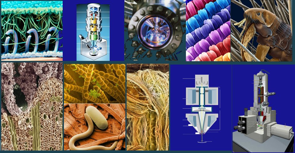

These three concepts all have the same abbreviations namely SEM, the Scanning Electron Microscope, the Structural Equation Model, and the Society for Experimental Mechanics, but that does not imply that they have the same meaning; in fact, each definition is entirely different from the other and falls within its own study field. What interests me most is the technology of Scanning Electron Microscopy. Ernest Ruska’s discovery of the electron microscope was a breakthrough invention in microbiology and greatly improved science. In modern society, the electron microscope is an essential tool in science and technology such as in engineering, foods and agriculture, forensics, maths, and in the medical field. Electron microscopy (especially scanning electron microscopy) has increasingly been applied for various purposes such as scientific experiments, forensic investigations, chemistry, electronics, and even space science. In diagnostics, it can differentiate diseased cells. In airline investigations, it can detect fatigued, fractured metals. In biology, it can inform about the discovery of new species, measure the impact of climate change on species, confirm the ultra-structure of cells and viruses, as well as verify new viruses and bacteria. In agriculture, it can detect the nature and structure of rock, the compilation of geological samples, and the quality of the soil for cultivation. Before I leap further into modern microscopy, I need to take you to the history of electron microscopes, how the Scanning Electron Microscope was invented, and what other inventions developed as a result of the Scanning Electron Microscopy/Microscope (SEM).
In 1590, a Dutch father and his son, Zach and Hans Janssen, invented the first light microscope. During that time in history a light microscope could magnify a sample up to a thousand times. The basis upon which a light microscope functions is that a light is released from a lamp; it then passes through a condenser lens before moving on to an objective lens (which can be regulated back and forth). An electron microscope functions differently in that it uses a beam to increase the speed of electrons as a source of light. As the wavelength of an electron can be hundred thousand times shorter than that of visible light photons, electron microscopes have higher resolute power than light microscopes; therefore, electron microscopes are able to expose smaller object structures than light microscopes. Also, electron microscopes use shaped magnetic fields to form sample images. The Scanning Electron Microscope (SEM) was invented in the early 1930s to overcome the limitations of light microscopes. It was originally invented to view non-biological materials such as metals. The electron microscope (also known as the Transmission Electron Microscope [TEM]) that used electrons instead of light to create the magnified image was invented in 1931 by a German electrical engineer, Ernst Ruska (1906 to 1988), who studied at the Technical University of Munich from 1925 to 1927. In 1933, an electron microscope was invented; based on the concept that electrons have a wavelength that is inversely comparative to their momentum. This electron microscope surpassed the magnifying limits of the optical microscope at the time. There were two basic types of electron microscopes; the transmission electron microscope and the scanning electron microscope (plus a hybrid of the two). In 1935, Max Knoll invented a Scanning Electron Microscope (SEM) with a 50 mm object-field-width that could channel contrast by the use of an electron beam scanner whereas conventional scanning electron microscopy depended on the emission of secondary electrons from the surface of the sample. Max Knoll’s SEM provided detailed images of the surfaces of cells and whole organisms that were not possible by TEM.
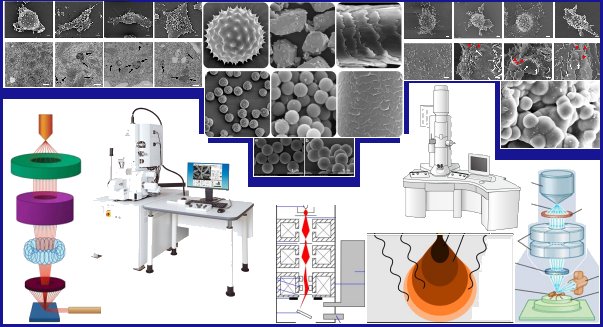
Apart from other parts that assist to monitor the sample such as power supply, a display device (computer), and anode (a positively charged plate), the Scanning Electron Microscope (SEM) consists of several main parts; an electron gun, lenses, a sample chamber, detectors, a vacuum chamber, and a scanning coil. The electron gun at the top of the microscope (in the upper part of the electron column) transmits electricity to an electron beam, generates electrons, and conveys them through the microscope. The scanning coil centralises the electron beam after emission from the electron gun before re-directing the beam onto two axes (this results in the sample being scanned after the last phase in the imaging process). Two or three magnet lenses under the electron gun bend the flow of electrons and condense the electron beam. The sample chamber collects the sample, stabilises it, moves it from one place to another, and positions it at different angles. The vacuum chamber inside the SEM is essential due to the fact that electrons are scattered by any aspect of light such as air and gases. In such a scenario (where electrons move away from the sample area), a vacuum pump is necessary to remove air and other gases from the vacuum chamber to create a vacuum. The detectors identify all electrons, change them into an electric current, convert the electric current into an image, and present the image onto a computer screen.
In 1937, Manfred von Ardenne invented a Scanning Transmission Electron Microscope (STEM) with a finely focused electron beam for high resolution three-dimensional images by scanning a very small raster with a de-magnified probe; before he discovered the STEM conventional electron microscopes were not able to scan three-dimensional images. 1951 provided the field ion microscope which was the first microscope that could view atoms. 1953 pushed the boundaries further with the invention of the phase-contrast microscope. In 1957, Marvin Minsky invented the con-focal microscope which had several advantages over conventional wide field optical microscopy such as the control of depth of field, reduction of background data of the focal area (which interfered with image clarity), and the ability to collect serial optical sections from thick specimens. Marvin Minsky’s invention was the forerunner of today’s con-focal laser scanning microscope. During the 1970s, a team of scientists at the Aerospace Corporation in California developed a technique to identify gunshot residue with the use of a SEM. Due to its extensive ability to examine and interpret detailed information of various materials, the SEM is a significant tool in modern forensic science. When analysing gunshot residue during investigation in a forensic laboratory, a SEM image is created of the residue as well as an X-ray spectrum to indicate a quantitative chemical analysis (in graph format). In 1981, Gerd Binnig and Heinrich Rohrer invented the Scanning Probe Microscope (also known as the scanning tunnelling microscope) that provides atomic level three-dimensional images. In 1986, half of the Nobel Prize for Physics was divided between Gerd Binnig and Heinrich Rohrer. Ernst Ruska was awarded the other half for inventing the electron microscope; mainly as a result of his pioneer project in Transmission Electron Microscopy (1931) and his later work in Electron Microscopy. Anton Van Leeuwenhoek invented the first convex lenses. He used microscopes to view various samples such as bacteria, blood cells, and pond organisms. With the invention of the thermal spray technique, industry and scientists became aware of the procedure’s potential to protect components against corrosion, heat, and wear; also, to acquire electrical and magnetic properties.
In 2016, physicist J.C. Séamus Davis noticed an elusive state of quantum matter when he discovered copper oxide materials connected to atoms. This launched a new sub-field in the study of quantum materials. Séamus Davis broke his own record by inventing the Scanning Josephson Tunnelling Microscope. Other discoveries followed until scientists could detect one atom at a time with the invention of a scanning probe microscope which transformed science fiction into reality and revolutionised nanoscience. Scanning Force Microscopy (SFM) or Atomic Force Microscopy (AFM) is an extremely high resolution probe microscopy method with the ability of imaging in nanometer scale at the molecular level. Today’s electron microscopes are able to observe the structure and morphology of a sample at a fraction of a nanometer.